


This article will describe the types of measurements and visual defects that can be acquired under the microscope. The optical technique most commonly used will be Brightfield Reflected Light; however other contrast techniques such as Darkfield, Polarized light and DIC can be used under certain circumstances. For example, DIC (differential interference contrast) can improve viewing of the copper grain structure and make the boundaries of multiple copper layers more easily defined.
With the increase in the layer count and decrease in the hole diameter, the implantation of microscopic cross-section analysis is critical for process control and failure analysis.
Here are many of the typical inspection issues and measurements used in cross-section analysis.
-
Voids
-
Plating Voids
-
Voids are non-plated areas in the walls of vias, and are one of the most common plating defects in through hole vias walls. A maximum void size is usually stated in quality specifications in order to avoid plating-voids producing functional failures.
- Plating voids are related to topographic abnormalities on the walls of the hole. Roughness of the wall could be caused by contaminants, air bubbles in the sides of the hole, or poor drilling.
-
Voids are non-plated areas in the walls of vias, and are one of the most common plating defects in through hole vias walls. A maximum void size is usually stated in quality specifications in order to avoid plating-voids producing functional failures.
-
Resin Voids
-
Voids in the dielectric laminant refer to the absence of epoxy resin in a circuit board.
- This can be caused by air bubbles, contaminates or many other issues. In addition to microscope reflected Brightfield for viewing, Darkfield contrast can be useful in detecting these defects.
-
Voids in the dielectric laminant refer to the absence of epoxy resin in a circuit board.
-
Delamination Voids
-
Delamination creates separation or gap in layers. There may be delamination of copper foil to core, or core to core.
- This type of defect often occurs relating to failure in the prepreg (adhesive material bonding two surfaces), although there are many types and causes for this type of problem. Eliminating voids in interfaces will greatly improve the quality of laminated structures. Again, Darkfield contrast may be of use here.
-
Delamination creates separation or gap in layers. There may be delamination of copper foil to core, or core to core.
-
Plating Nodules
- These are raised areas or bumps protruding from the via wall. This can cause plating variation and stress in that location. This can be caused by several problems such debris attached to the wall prior to plating or glass fibers exposed during etch back process just to name a couple. Nodules can reduce PCB life when being used in extreme environmental conditions.
-
Plating Voids

-
Etchback (Positive and Negative)
- Negative etchback features inner copper layers retreating from the edge of the hole wall. The amount must be controlled to meet manufactures specification.
- Positive PCB etchback removes resin and fibers from the hole wall and displays the copper traces protruding from the crossed edge of the hole walls, providing a solid contact to plating. Manufacturers often apply positive etchback in high-reliability multilayer PCB in the medical, aerospace, and military systems.

-
Plating Corner Cracking (knee)
- These cracks appear on the knee of the plated through hole. During manufacturing poor plating can be caused by the quality of the materials used (e.g., contaminants). Corner cracking can also appear after thermal treatment.

-
Registration of drill hole
-
Alignment of layers during stack up and the proper design distances of tracks and vias ensure drill holes hit the bullseye in each layer. Yet process variations and other issue may produce misalignment and off-center drill holes which can produce lower performance and reliability, and in worst cases create breaks in connection.
- Cross-section viewing of the via can indicate proper hole placement in the copper pad. Measurement of copper width on either side of the hole can confirm proper hole placement within the specifications.
-
Alignment of layers during stack up and the proper design distances of tracks and vias ensure drill holes hit the bullseye in each layer. Yet process variations and other issue may produce misalignment and off-center drill holes which can produce lower performance and reliability, and in worst cases create breaks in connection.
-
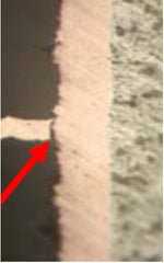
Resin smear
-
A resin smear is the epoxy resin substrate being deposited over the internal copper layer during the via hole drilling process. This smear of epoxy can cause the plating to not make contact with the copper layers.
- The process of “desmearing” by etching can be used to remove debris and the epoxy resin that has melted and been dragged over the copper layers hence creating contact between layer trace and wall plating.
-
A resin smear is the epoxy resin substrate being deposited over the internal copper layer during the via hole drilling process. This smear of epoxy can cause the plating to not make contact with the copper layers.
-
Throwing Power (%)
-
Throwing power (%) is basically a ratio of plating wall thickness to plating thickness on top and bottom of via. This is greatly affected by the aspect ratio of the via’s height to its diameter.
- Process control needs to meet the desired % (usually >80%). Typically, the plating thickness measurement on the wall of the via is taken in 3 locations (25%, 50% and 75% down the hole).
-
Throwing power (%) is basically a ratio of plating wall thickness to plating thickness on top and bottom of via. This is greatly affected by the aspect ratio of the via’s height to its diameter.

-
Thickness measurements
- For cross-section measurement using a microscope and digital camera, the proper selection of contrast technique is usually brightfield reflected light. In addition, it is important to consider the proper magnification for the thickness range of interest. Low magnification allows a larger field of view; however, the object of interest may only cover a small number of pixels on the digital camera leading to poor accuracy and precision. Increasing magnification provides a larger number of pixels with better more reproducible results. Software features like tiling would be helpful in providing a large field of view, while maintaining high magnification.
-
A few of the areas where measurements may be needed:
- Copper film thickness
- Copper deposited on top and bottom land regions
- Basic copper on top and bottom land regions
- Copper plating thickness variation on barrel wall
- Inner layer copper thickness
- Corner (knee) plating thickness
- Dielectric layer thickness
- Solder thickness
- Solder mask thickness
- Barrel diameter
Motic’s family of microscopes provides ideal solutions for the inspection of the defects mentioned above.

|
The PA53MET is an upright microscope that holds brightfield, darkfield, polarization and DIC options along with easy-to-use software for measurement and recordkeeping. The microscope also offers motorized xyz for more advanced imaging applications. |
|---|
 |
The PX43MET is an inverted materials microscope that features Brightfield, Darkfield, and Polarization. But unlike most inverted microscopes at its price range, it also features DIC, which adds incredible depth and elevated features to your imaging. This reflected light inverted scope is great for looking at prepared cross-sectioned samples, or large metal, die cast parts that are too large to view under a conventional upright microscope. |
|---|
In our other article, we talk about sample preparation for PCBs and the pros and cons of using upright and inverted microscopes.
Leave a note for our applications team if you are interested in learning more - either through a demo, a pricing quote or just additional brochures.