


Wafer inspection in the semiconductor industry is a complicated, multistage process. In this two part series, our experts at Motic will outline the basics of the inspection process, and how light microscopes can help during optical analysis.
Fundamentally, wafer inspection is split into two categories: unpatterned and patterned wafers. Generally, unpatterned inspection looks at defects on bare wafers. Patterned inspection looks at defects on processed wafers now containing circuitry.
Following our last article on unpatterned wafers, today we’ll be looking at patterned wafer inspection and how material microscopes should be used in this process.
Patterned Wafer

Patterned wafers, during the step-by-step processing, pose complex possibilities of defects. In the many process steps of building up, layer by layer, a 3-dimensional circuit containing many different materials, many defect types can be fatal. Here too light microscopy has been a common tool to inspect and identify many of the defects associated with the fabrication process.
Below are some examples of inspection and defects seen in patterned wafers:
Mouse Bites, which are a narrowing of a section of an interconnect (conductor), “Opens” along interconnects and Bridging, which is a short circuit between to active areas/interconnects.
Most of these types of defects can be viewed in Brightfield contrast.

Residual Photoresist /Scumming is the material left behind after etching or other processes. It can be a small or thin area of photoresist which can be hard to visualize in Brightfield and Darkfield contrast.
Utilizing Fluorescence contrast can produce a “glowing” area of the residual resist for easy inspection.
Scratches may have come about due to mishandling and malfunctioning equipment. This can be a killer defect.
Scratches may be very fine in both lateral and depth dimensions and often not observed well in Brightfield contrast. Darkfield contrast provides an advantage since it utilizes scattered light from edges to provide a bright scratch on the patterned background.
The DIC contrast (differential interference contrast) technique can be useful since it can produce a change in contrast with a change in depth and can be sensitive in the nanometer topographic range.
However, DIC is a single shear directional (azimuth) technique and has maximum contrast with scratch perpendicular to its direction, while having very low contrast when the scratch is parallel.

Surface contaminants (particles) which are typically foreign material on the patterned wafer are in most cases “critical” defects which will make the semiconductor wafer useless. These particulates come in many shapes, sizes, colors and materials.
Brightfield contrast will make many of these particles visible however some particles (e.g., transparent material) may not be easily seen.
Darkfield contrast can be a big help in visualizing most particles, even those that are transparent since this contrast method uses scattering effects to make objects visible down to submicron size.
Light scattering from the particles can produce a bright spot on the patterned wafer.

Transparent films/coatings may have defects such as pits and localized stress which may cause circuit malfunction in the near or long term.
Here again Darkfield may detect pits or voids in such films. For the visualization of localized stress, the use of Crossed Polarized Light contrast may be best.
Dimensional measurement for circuit features (CD-critical dimension). This is typically line width measurement of interconnect conductors, etc.
Brightfield contrast with encoded software is often the most used contrast technique for simple measurements. Naturally, other more dedicated instruments are used for high accuracy applications.
Surface variation of Mentalization (e.g., interconnects, pond pads, etc.) can be of interest for process control.
DIC contrast is a very useful tool to see what the surface looks like (smooth, rough, pits). It provides a relief image of the surface topography.

Inspection of multiple layers can sometimes be difficult. Understanding what layer is where in the image is not always clear.
The optical sectioning capability of DIC can produce a clearly focused image of a layer while other layers are defocused. This provides an understanding of what parts of the image are on the same plane.
Refocusing gives the same to the next level, etc. This is more focus sensitive than standard Brightfield contrast.
The optical section property of DIC can aid in understanding what is part of each layer in a semiconductor device. (below image is from the Nikon Microscopy University website)

Motic’s PA family of microscopes is an ideal solution for the inspection of the defects mentioned above.
 |
The PA53MET holds all brightfield, darkfield and DIC options along with easy-to-use software for measurement and recordkeeping. The microscope also offers motorized xyz for more advanced imaging applications. |
|---|
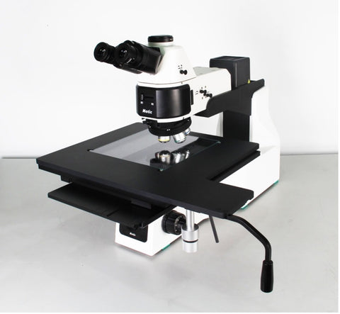 |
The PA120MET solution below offers a 12 inch stage for larger wafers, with a pistol grip for quick and easy examinations across the entire stage. It offers the same contrasting methods as the PA53MET, with brightfield, darkfield and DIC options as well. |
|---|
Leave a note for our applications team if you are interested in learning more - either through a demo, a pricing quote or just additional brochures.